Guizhou Huoying Technology Co., Ltd.
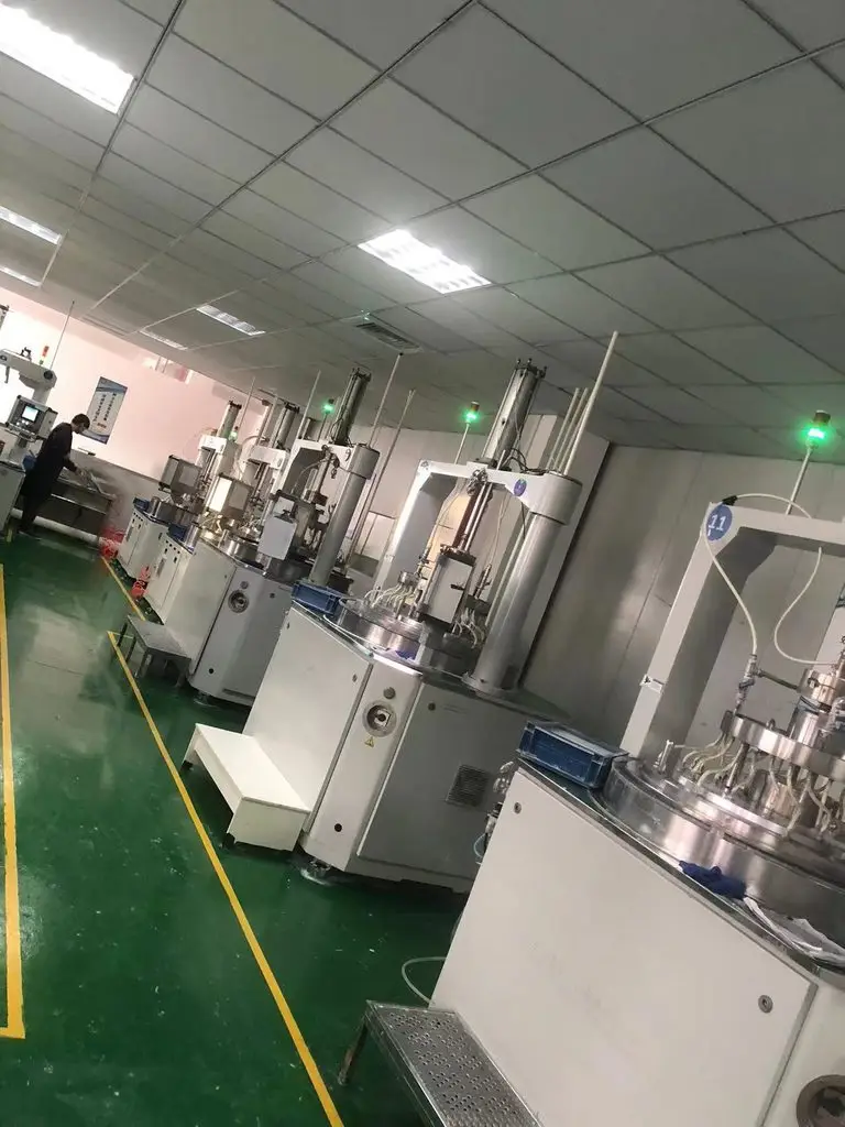
Guizhou Huoying Technology Co., Ltd. is a professional supplier focusing on semiconductor and optoelectronic substrate materials, located in Guizhou, China. We integrate material processing, technical consultation and global export sales, serving semiconductor fabs, research institutes, universities and optoelectronic enterprises worldwide.
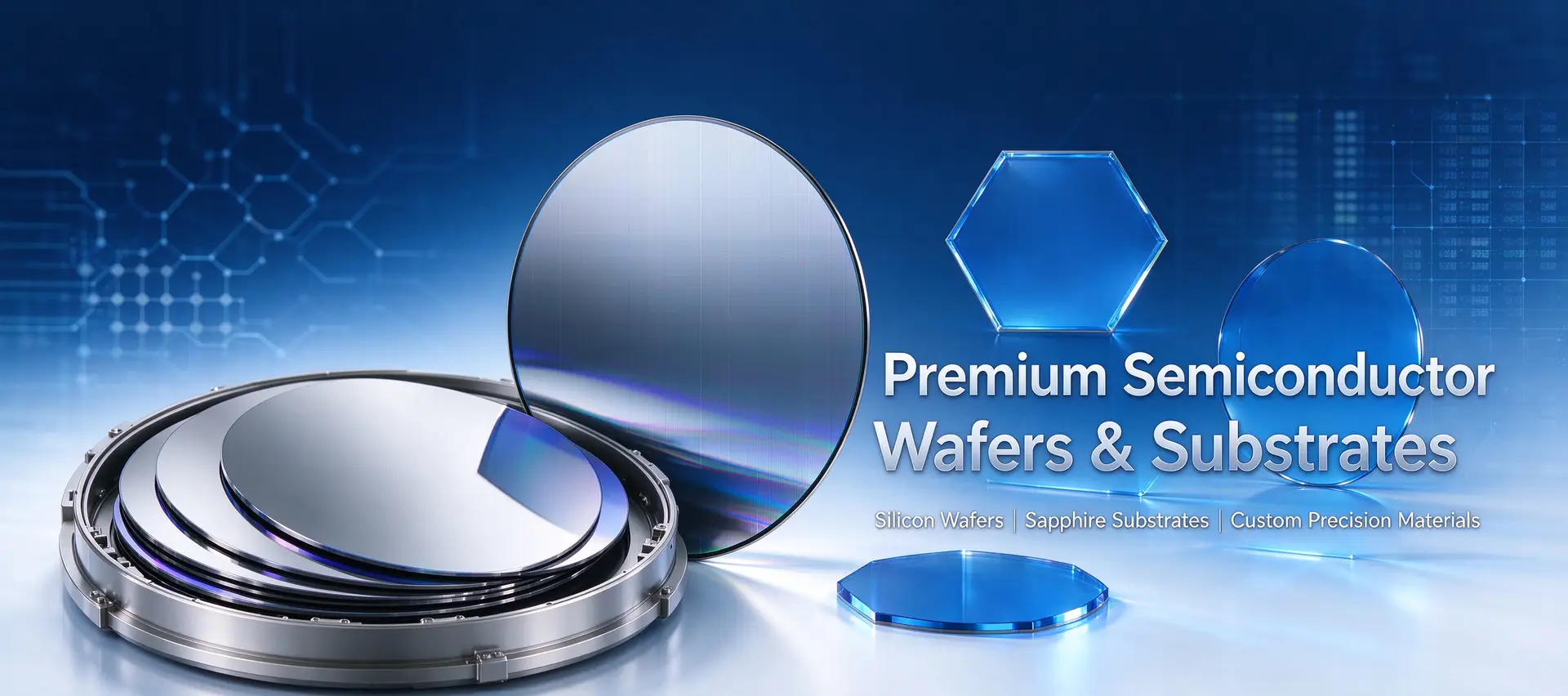
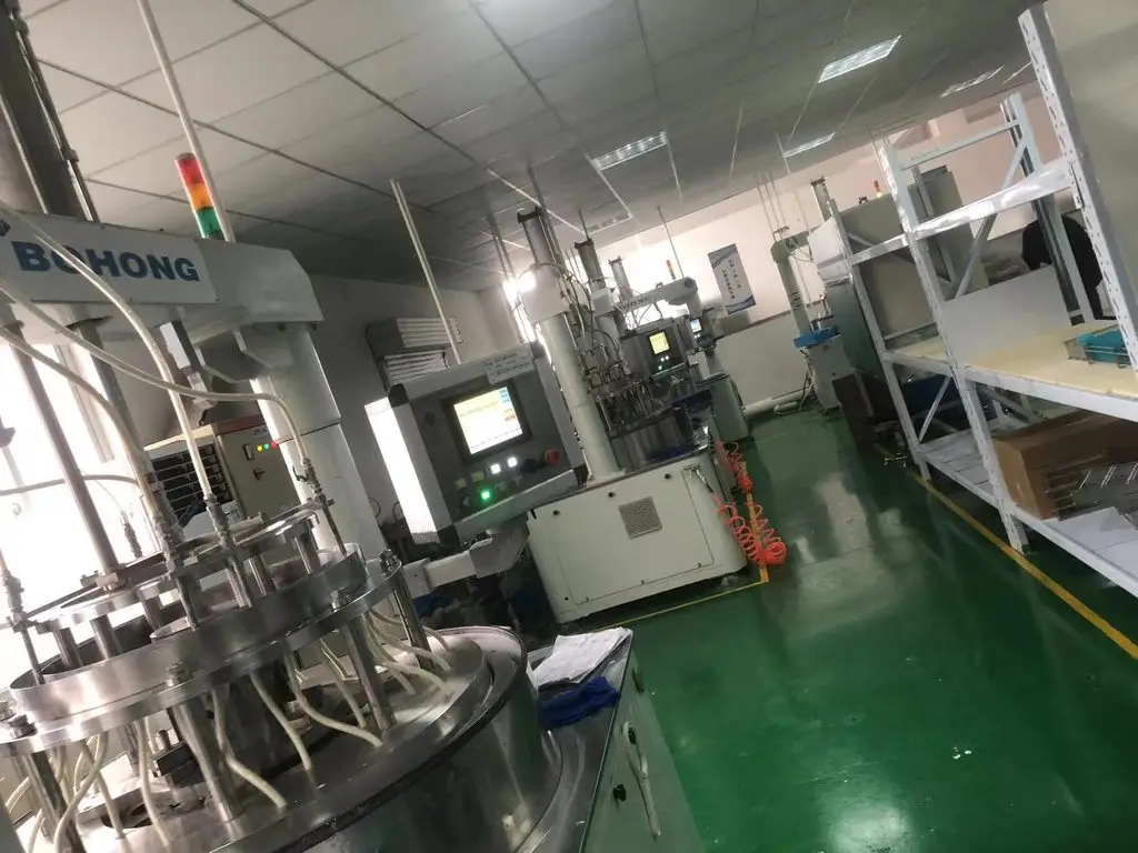
Our product portfolio covers a full range of semiconductor wafers and optical substrates, including silicon wafers, SiC substrates & wafers, sapphire substrates, GaN, GaAs, InP, germanium wafers, ZnSe, YAG crystal, BF33 optical glass wafers and other specialty optical window materials. We can customize crystal orientation, thickness, TTV, Warp/Bow, doping type and surface polishing specifications according to customer drawings and technical requirements, and provide cutting, thinning, coating and other precision processing services.
Why Choose Us
✅ Diverse Material Portfolio: Cover silicon, wide-bandgap semiconductor and infrared optical crystal materials
✅ Custom Precision Machining: Adjustable crystal orientation, flatness, thickness, polishing and coating
✅ Complete Quality Documentation: COA, inspection data, TTV/Warp/Bow test records available
✅ Flexible Order Support: Sample, small batch and volume orders accepted, no rigid high MOQ
✅ Professional Technical Team: Fast response for wafer specification consultation and technical problem solving
✅ Global Export Service: Rich experience on international logistics, customs and foreign trade documentation
Our advantages
We strictly follow SEMI industrial standards for quality control. Every batch of products is inspected with complete test reports and COA certification. We support small batch sampling, R&D prototype orders and mass production supply, flexible MOQ to meet different demands from laboratory research to industrial mass manufacturing.
Adhering to the principle of Quality First, Customer Centric, Integrity & Win-Win Cooperation, Huoying Technology is committed to becoming your reliable long-term partner for semiconductor substrate materials. We keep optimizing our supply chain and processing capability to help global customers solve material procurement and customized processing challenges.