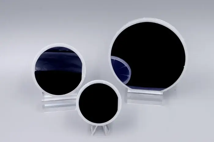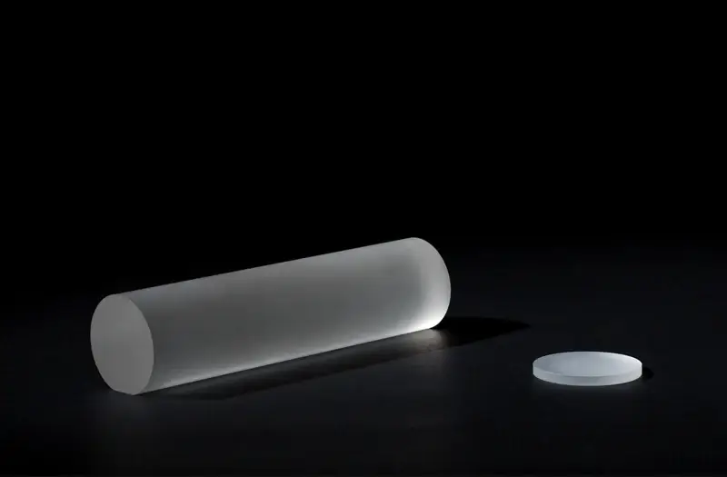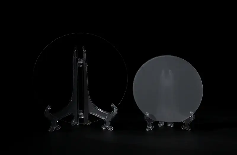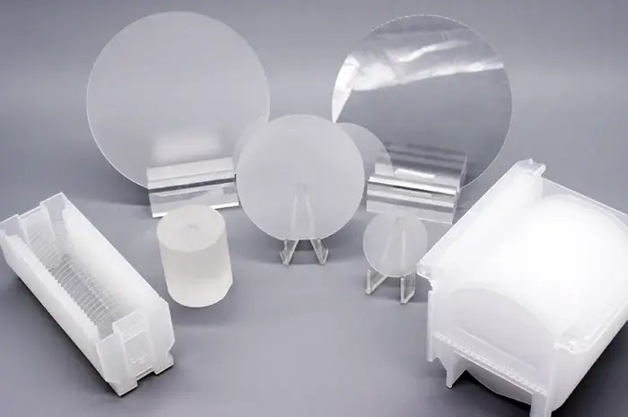

We supply high‑quality 2‑inch C‑plane (0001) double‑side‑polished (DSP) sapphire substrates, also known as Al₂O₃ monocrystalline sapphire wafers. Two mainstream thickness options are available: 100 μm ultra‑thin version and standard 430 μm version. These DSP sapphire wafers feature ultra‑low surface roughness, excellent flatness and precise crystal orientation, widely used for GaN epitaxy, LED chip manufacturing, semiconductor research, and optical device development. Single‑side polished (SSP) sapphire wafers can also be provided upon request.
Contact us for quotation: WhatsApp / Tel: +86‑13262739223
Specification Sheet
Document Name: 2inch C‑plane (0001) DSP Sapphire Substrates Version: A/0 Material: Monocrystalline Sapphire (Al₂O₃)
1. Shape & Dimension Parameters (Unit: mm)
| No. | Item | Target Value | Tolerance | Remark |
|---|---|---|---|---|
| 1 | Diameter | 50.8 mm | ±0.2 mm(100μm);±0.1 mm(430μm) | 2‑inch standard size |
| 2 | Thickness | 100 μm / 430 μm | ±15 μm | Two thickness grades optional |
| 3 | Surface Orientation
(Off‑axis towards M‑plane) |
0.2° | ±0.1° | C‑plane (0001) miscut |
| 4 | Primary Flat Length | 16 mm | ±1 mm | SEMI standard flat |
| 5 | Primary Flat Orientation | C‑plane | ±0.1° | |
| 6 | Back‑side Surface Roughness Ra | < 0.3 nm | ‑ | Double‑side polished |
| 7 | Front‑side Surface Roughness Ra | ≤0.3 nm(DSP);
1.0±0.2 μm(SSP) |
‑ | DSP: double side polished;
SSP: single side polished |
| 8 | Wafer Edge Profile | R‑type | ‑ | Chamfered edge for chip processing |
| 9 | TTV (Total Thickness Variation) | ≤ 10 μm | LTV ≤ 5 μm @5×5 mm scan | Total thickness variation |
| 10 | Warp | ≤ 10 μm | ‑ | Whole‑wafer warp value |
| 11 | Bow | ‑10 μm ≤ Bow ≤ 0 μm | ‑ | Concave‑type bow control |
| 12 | Laser Mark | N/A | ‑ | No laser marking |
Packing & Traceability
- Packing: 25 pieces per standard wafer cassette
- Traceability: Each batch of sapphire substrates can be fully traced by cassette number.
- Custom specifications, alternative orientations (A‑plane, M‑plane, R‑plane), custom thickness and miscut angles are acceptable.
Application
- LED epitaxy & GaN thin‑film growth
- Semiconductor laboratory research
- Laser diode manufacturing
- Optical‑infrared components
- Heterogeneous material deposition experiments