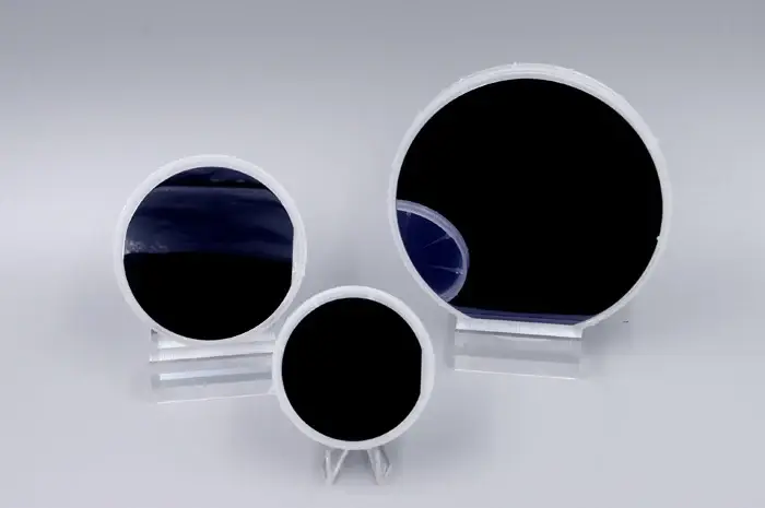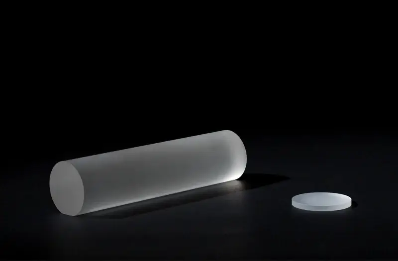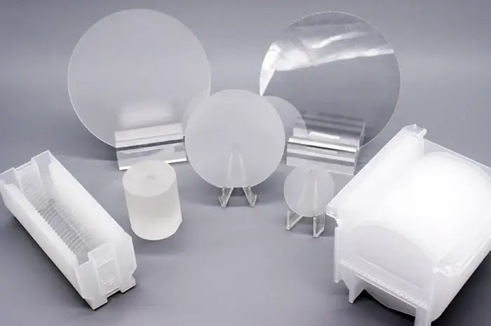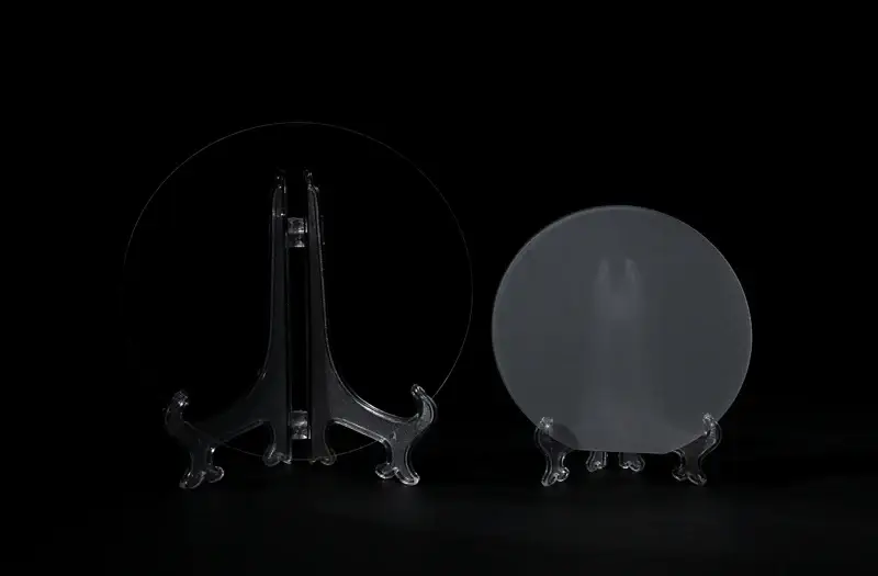
1. What is GaAs Substrate & GaAs Wafer? Main Applications
Gallium Arsenide (GaAs) is a high‑performance compound semiconductor material, featuring direct band‑gap, high electron mobility, high‑frequency & low‑noise performance, and high conversion efficiency.
GaAs substrates are available in conductive type and semi‑insulating type. They are widely adopted for:
- Laser Diodes (LD), LED chips, near‑infrared lasers, quantum‑well high‑power lasers, high‑efficiency solar panels
- HEMT & HBT chips for radar, microwave, millimeter‑wave systems and ultra‑high‑speed computing & optical communication
- RF components for wireless communication, 4G / 5G, satellite communication and WLAN systems
Recently, GaAs substrates have achieved great progress in Mini‑LED, Micro‑LED and red‑light LED sectors, and are extensively deployed for AR / VR wearable devices.
2. GaAs Substrate Specifications
| Item | Parameter |
|---|---|
| Diameter | 50mm | 75mm | 100mm | 150mm |
| Growth Method | LEC (Liquid‑Encapsulated Czochralski), VGF (Vertical Gradient Freeze) |
| Wafer Thickness | 350 μm ~ 625 μm |
| Crystal Orientation | <100> / <111> / <110> or custom orientations |
| Conductive Type | P‑type / N‑type / Semi‑insulating |
| Dopant | Zn / Si / Undoped |
| Carrier Concentration | 1E17 ~ 5E19 cm⁻³ |
| Room‑temperature Resistivity (SI grade) | ≥1E7 ohm•cm |
| Electron Mobility | ≥4000 cm²/V·sec |
| EPD (Etch Pit Density) | 100 ~ 1E5 cm⁻² |
| TTV (Total Thickness Variation) | ≤ 10 μm |
| Bow / Warp | ≤ 20 μm |
| Surface Finish | DSP (Double‑Side Polished) / SSP (Single‑Side Polished) |
| Laser Mark | Available upon request |
| Grade | Epi‑polished grade / Mechanical grade |
Customization: Custom thickness, polishing and lapping grades are available according to customer requirements.
3. GaAs Epitaxial Wafer Specifications
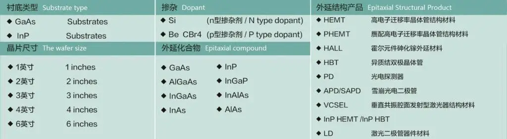
We provide custom‑built GaAs epitaxial wafers with varied epitaxial structure and thickness. Our GaAs epi‑wafer product portfolio covers multiple device‑oriented structures for optoelectronic and RF applications.
Related products: GaAs substrate, InP substrate, GaN substrate 4‑Inch Custom Ultra‑Thick Silicon Wafers|Custom Ultra‑Thin & Ultra‑Flat Silicon Wafers 磷化铟单晶衬底