1、What is Special‑Orientation Sapphire Substrate?
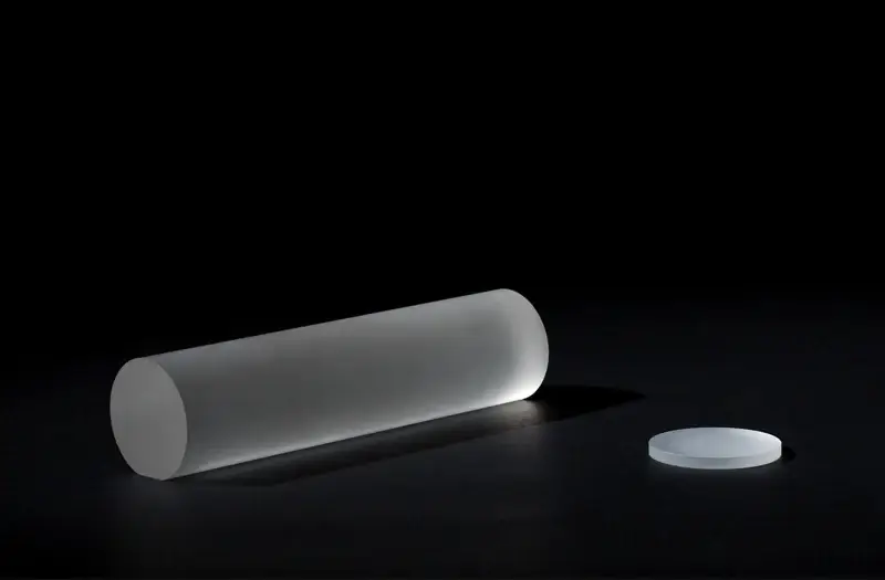
Special‑orientation sapphire substrates refer to A‑plane, M‑plane, R‑plane, N/V‑plane and other orientations deviating from conventional C‑plane (0001), as well as small‑angle off‑cut / miscut sapphire wafers.
These substrates can precisely control crystal polarization, lattice matching, internal stress and surface step morphology. They serve as foundational carriers for high‑performance epitaxy of non‑polar / semi‑polar GaN, two‑dimensional materials, radio‑frequency components and optoelectronic devices.
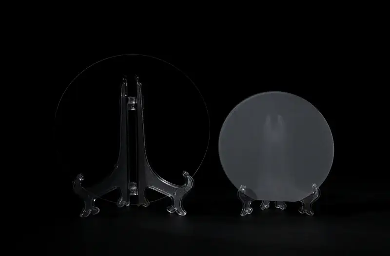
Specifications of A‑M‑R Sapphire Monocrystal Substrates (2‑6 inch)
| Item | Parameter |
|---|---|
| Material | >99.99% High‑purity monocrystalline Al₂O₃ (KY method) |
| Crystal Orientation | A‑plane (11‑20) ±0.1°;R‑plane (1‑102) ±0.1°;M‑plane (1‑100) ±0.1° |
| Diameter | 50.8 mm (2”), 100 mm (4”), 150 mm (6”) |
| Thickness | 430 μm (2”), 650 μm (4”), 1000 μm (6”) |
| Primary Flat Orientation | A‑plane wafer: M‑plane ±0.3°;
R‑plane wafer: Counter‑clockwise 45° from C‑axis; M‑plane wafer: A‑plane ±0.3° |
| Primary Flat Length | 16 mm (2”), 30 mm (4”), 47.5 mm (6”) |
| Front Surface | Epi‑polished, Ra<0.3 nm |
| Back Surface | SSP: Fine‑ground, Ra=0.8‑1.2 μm;DSP: Epi‑polished, Ra<0.3 nm |
| TTV(Total Thickness Variation) | <10 μm (2”);<20 μm (4”);<25 μm (6”) |
| BOW | ‑15~0 μm (2”);‑25~0 μm (4”);‑35~0 μm (6”) |
| WARP | <15 μm (2”);<30 μm (4”);<40 μm (6”) |
| Edge Exclusion | ≤2 mm |
Mainstream Special Crystal Orientation Comparison
- A‑plane (11‑20): Prismatic face, non‑polar orientation. Well‑defined surface atomic steps, strong birefringence, uniform dielectric property and excellent insulation performance.
- M‑plane (10‑10): Main prismatic face, non‑polar orientation. Free of spontaneous polarization to suppress QCSE effect; high mechanical strength and uniform etching performance.
- R‑plane (1‑102): Rhombohedral face, semi‑polar orientation. Superior lattice matching with Si/GaN, low thermal stress, ideal for heterogeneous epitaxy.
- N‑plane (11‑23) / V‑plane (22‑43): High‑index semi‑polar planes. Adjust GaN polarization and crystal curvature; widely used for long‑wavelength LED and LD.
- Off‑cut / Miscut: C/A/M‑plane with 1°‑10° offset (common 2°,4°). Generate ordered atomic steps on wafer surface, eliminate anti‑parallel domains and improve monocrystalline quality of epitaxial layers.
Performance & Application Comparison Table for Different Orientations
| Crystal Orientation | Polarity | CTE (⊥c‑axis, ×10⁻⁶/K) | Surface Feature | Typical Epitaxy Application |
|---|---|---|---|---|
| A‑plane (11‑20) | Non‑polar | ~7.5 | Regular atomic steps, anisotropic | Non‑polar GaN, 2D‑material growth |
| M‑plane (10‑10) | Non‑polar | ~7.0 | Zero polarization field, low defect density | Green LED, UV photodetector |
| R‑plane (1‑102) | Semi‑polar | ~8.0 | Good lattice‑match, low stress | Silicon heterogeneous epitaxy, power devices |
| C‑plane +2° miscut | Polar | ~8.3 | Unidirectional atomic steps, no domain wall | Wafer‑scale MoS₂, AlN epitaxy |
Our Advantages
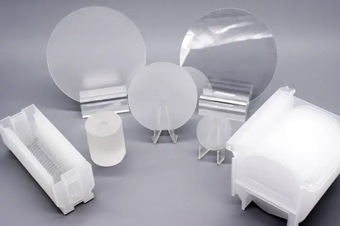
We supply various grades of special‑orientation sapphire substrates including A‑plane, M‑plane, R‑plane and miscut sapphire wafers. Custom processing and mass‑volume supply are available.
Our epi‑ready sapphire wafers are strictly inspected for surface roughness, flatness, bow & warp before delivery, stable for laboratory R&D and mass‑production epitaxy projects.
For quotation and technical datasheet, please contact us via WhatsApp / Email.