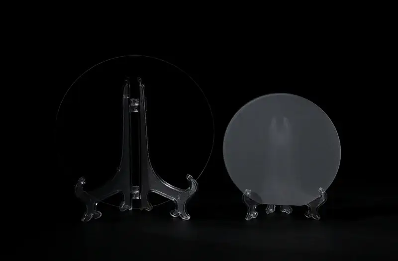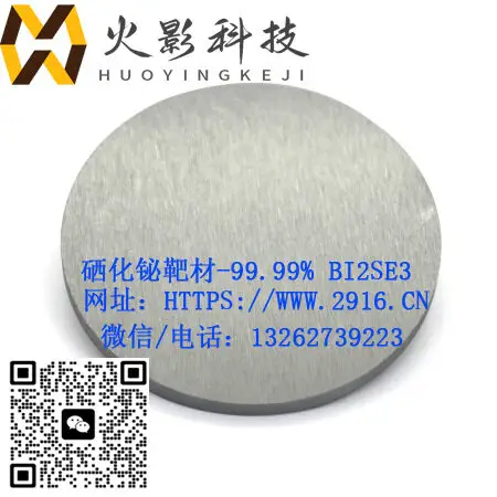

一、What is 4N Bismuth Selenide Sputtering Target?
4N Bismuth Selenide (Bi₂Se₃) sputtering target is a polycrystalline chalcogenide ceramic sputter target widely used for scientific magnetron sputtering experiments. As a classic three‑dimensional topological insulator material, it is highly demanded in quantum material and spintronics research。
- Chemical Formula:Bi₂Se₃
- CAS Number:12068‑69‑8
- Purity:99.99% (4N), tested via GDMS analysis
- Total metallic impurity: <100 ppm
- Strictly controlled defects: Se‑vacancy, Bi segregation; low O, C, Fe, Cu, Te impurities
- Crystal Structure: Hexagonal‑rhombohedral (R‑3m), quintuple‑layer (QL) stacking structure
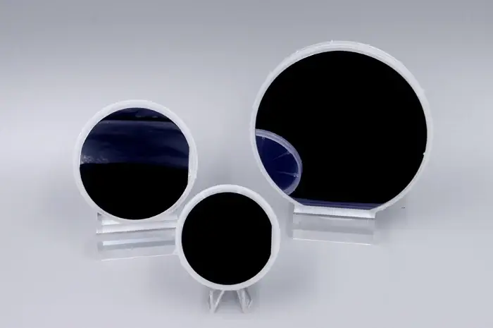
- Appearance: Grey‑black brittle ceramic bulk
- Theoretical Density: 6.82 g/cm³
- Relative density of sintered target: 94‑97%
- Melting Point: 706‑710 ℃ ~ 710 ℃
- Material features: Prone to selenium volatilization and compositional mismatch; low thermal conductivity, thermal‑shock sensitive, high brittleness
- Electrical property: Intrinsic 3D topological insulator with bulk band gap ~0.3 eV; normally presents n‑type conduction caused by selenium vacancies; medium resistivity, not suitable for DC sputtering
2: Key Process Notes for Bi₂Se₃ Sputtering
Bi₂Se₃ ceramic target has special sputtering requirements due to selenium volatility and ceramic brittleness. Please strictly follow below operation guidelines:
- Only 13.56 MHz RF magnetron sputtering is allowed; DC sputtering is forbidden. Direct‑current mode will trigger surface charging, arcing and severe compositional drift of thin‑film.
- Selenium is easy to evaporate under high temperature. Keep low target‑surface temperature; increase sputtering power gradually instead of sharp high‑power input. Minor selenium atmosphere or high‑purity N₂ can be adopted to mitigate Se loss, with Ar as primary working gas. Se‑vacancy defects commonly cause heavy n‑type doping in deposited Bi₂Se₃ thin films.
- Low thermal conductivity makes the target vulnerable to cracking under thermal shock. Ensure good water‑cooling for backing plate. Handle with care for its high brittleness.
- Bismuth selenide is prone to oxidation and moisture absorption. Store target under vacuum environment. Wear cleanroom gloves during handling. Long‑term air exposure degrades surface quality and destroys film stoichiometry.
3: Alternative Deposition Solutions Comparison
| Solution | Advantages | Drawbacks |
|---|---|---|
| Bi₂Se₃ ceramic target (RF sputtering) | Direct thin‑film deposition | High risk of Se volatilization & composition deviation; relatively high target cost |
| Bi target + Se co‑sputtering / co‑evaporation | Independently tune Bi & Se flux | Higher equipment complexity |
Safety Warning: Bismuth selenide is toxic selenide substance (UN3283, Class 6.1 toxic material). Avoid inhaling grinding dust and target debris. Waste targets must be disposed as toxic inorganic compound waste.
4、Performance Comparison with Typical Ceramic Sputtering Targets
| Item | Bi₂Se₃ | GaN | Cr₂O₃ |
|---|---|---|---|
| Material Type | Chalcogenide topological insulator | Nitride wide‑bandgap semiconductor | Metal‑oxide insulating ceramic |
| Recommended Power Source | RF | RF | RF |
| Main Risks | Se volatilization & compositional mismatch, thermal‑shock cracking | High‑temperature decomposition & nitrogen loss | Thermal‑shock cracking |
| Typical Applications | Topological insulator & spintronics research | Optoelectronic & power‑device R&D | Wear‑resistant coating, optical & antiferromagnetic thin‑films |
5、Main Applications of Bismuth Selenide Bi₂Se₃ Sputtering Target
- Topological Insulator Thin‑films (Core Application) Produce Bi₂Se₃ topological insulator thin‑films for quantum‑material research, spintronics, ARPES measurement and transport‑property devices, investigating Dirac surface states.
- Optoelectronic & Infrared Photodetector Devices For broadband photodetection and nonlinear optical thin‑film studies.
- Thermoelectric Thin‑film Research Research on Te‑free thermoelectric materials with lower toxicity compared with Bi₂Te₃ systems.
- Heterostructure & Superconductor‑Topology Composite Films Low‑dimensional device fabrication and frontier condensed‑matter physics research.
6: Custom & Support Service
We can provide Bi₂Se₃ sputtering targets in custom dimension, shape and backing‑plate bonding for lab R&D. Contact our sales team for quotation and specification confirmation.
Related Products You May Also Interest: High‑purity Titanium Sputtering Target 4N5, Cobalt Sputtering Target 99.95%, 4‑inch P‑type <111> Silicon Wafer, InSb Single Crystal Wafer, C‑Plane Sapphire Substrate.