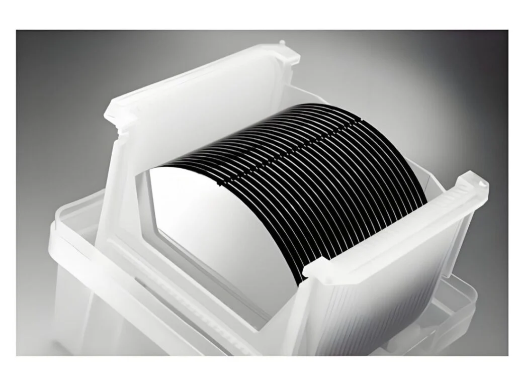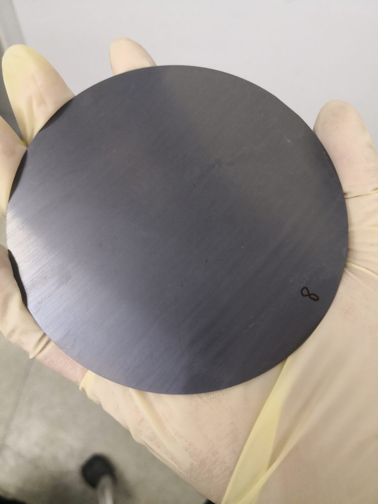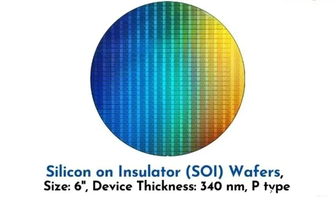

As semiconductors evolve toward higher integration, lower power consumption and better device performance, Silicon‑On‑Insulator (SOI) wafers stand out as core substrates for post‑FinFET chip manufacturing. Featuring a unique buried silicon‑dioxide insulating layer, SOI substrates become the preferred material for 5G RF front‑end modules, automotive electronics, AI chips and quantum computing devices.
Compared with conventional bulk silicon wafers, SOI wafers eliminate parasitic capacitance and suppress leakage current, delivering significant improvements for semiconductor component performance.
1. SOI Wafer Structure & Core Technical Parameters
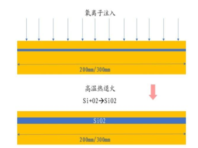
SOI wafer adopts a classic silicon‑insulator‑silicon sandwich structure. The top silicon (device layer) builds transistors; the middle buried oxide (BOX) layer electrically isolates devices from the bottom substrate; the bottom silicon handle layer offers mechanical support. Full dielectric isolation solves leakage and crosstalk issues caused by parasitic PN junctions in bulk‑silicon devices.
Key Performance‑Driving Parameters
SOI performance is mainly determined by three indicators: top silicon device‑layer thickness, buried oxide(BOX) thickness and crystal defect density. Precise control directly defines switching speed, power consumption and integration density of final chips.
- Top Silicon (Device Layer) Thickness
- FD‑SOI (Fully‑Depleted SOI): Top silicon thickness 5‑20 nm (for 28 nm and below process nodes), realizing full depletion and suppressing threshold‑voltage drift.
- RF‑SOI (Radio‑Frequency SOI): Typical device‑layer thickness 100‑300 nm, balancing RF signal transmission efficiency and parasitic capacitance for wireless circuits.
- Buried Oxide (BOX Layer) Thickness
- FD‑SOI: BOX thickness 20‑50 nm for low substrate capacitance
- RF‑SOI: BOX thickness 100‑200 nm for superior RF isolation performance
- Crystal Defect Density Electronic‑grade SOI wafers require defect density <100/cm², far stricter than bulk‑silicon standards (<1000/cm²), to guarantee transistor reliability.
Manufacturing Technology: Smart‑Cut Process
Modern SOI wafers are mass‑produced by the proven Smart‑Cut layer‑transfer technology:
- Hydrogen ion implantation into donor silicon wafer to form cleavage layer
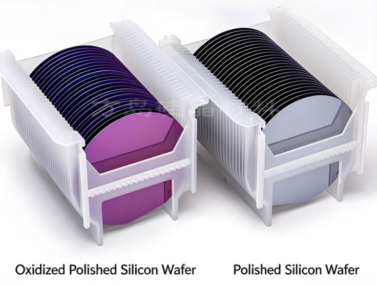
- Bond donor wafer with oxidized silicon handle wafer
- Mechanical stress induced layer splitting to transfer thin top silicon onto handle substrate
- CMP chemical‑mechanical polishing to achieve atomic‑level flatness (Surface roughness Ra < 0.5 nm)
Smart‑Cut supports high yield (>95%) and large‑size production up to 300 mm (12‑inch), meeting requirements for high uniformity substrates for 5G, AI and advanced semiconductor R&D.
2. Main Application Fields of SOI Wafers
Thanks to low‑power, high‑integration and high‑reliability characteristics, SOI substrates are widely deployed across RF wireless, automotive electronics, artificial‑intelligence chips and quantum‑computing research.
2.1 5G RF Front‑End | RF‑SOI
RF‑SOI is a key substrate material for modern 5G RF front‑ends.
- High isolation>50 dB to prevent signal crosstalk
- Low insertion loss (<0.8 dB) for high‑efficiency RF signal transmission
- Full CMOS‑process compatibility; RF switches, LNA and tuners can be monolithically integrated on one chip for lower packaging cost.
Over 90 % of global 5G RF switches adopt RF‑SOI substrates for smartphone and wireless‑communication hardware.
2.2 Automotive Electronics | Power‑SOI
Power‑SOI targets automotive requirements: high‑voltage endurance, wide‑temperature‑range reliability and high operating temperature resistance.
- Breakdown voltage>1200 V for motor control and BMS battery‑management circuits
- Buried oxide eliminates parasitic PN‑junction leakage under high‑temperature conditions (>150 ℃), extending device service life over 10 years
- Enables monolithic integration for power circuits & control logic, shrinking PCB footprint by around 50 % and reducing system‑level costs.
Power‑SOI substrates are widely used for AFE analog front‑end chips inside electric‑vehicle battery‑management systems.
2.3 AI Chips | FD‑SOI
FD‑SOI delivers advantages for low‑power high‑performance AI computing chips:
- Static power consumption reduced up to 70 % (28 nm node) by leakage‑current suppression
- Higher integration density (30 % improvement vs traditional FinFET solutions)
- Back‑biasing technique simplifies chip design flow and lowers development cost for AI accelerators.
2.4 Quantum‑Computing Research
The buried oxide layer of SOI wafer provides excellent electrical isolation for quantum‑bit devices. SOI substrates effectively reduce quantum‑bit crosstalk and extend quantum coherence time compared with bulk‑silicon wafers, widely adopted for lab quantum‑computing prototype research.
3. Market Outlook
Driven by 5G communication, electric‑vehicle and AI industries, global SOI wafer market keeps steady growth. Large‑size (300 mm /12‑inch), high‑performance SOI wafers become mainstream. Beyond RF, automotive and logic chips, SOI substrates expand rapidly into silicon photonics, MEMS sensors and optoelectronic‑device markets.
4. Our Offer
We supply customizable SOI wafers including RF‑SOI, FD‑SOI and Power‑SOI. Multiple diameters (2″‑12″), tunable device‑layer & BOX thickness, N‑type / P‑type doping options are available for commercial mass‑production and scientific research projects.
Send us your specification requirements for quotation.
FAQ
Q: What is SOI wafer used for?**
A: SOI wafers serve as advanced semiconductor substrates for 5G RF front‑end modules, automotive power chips, low‑power AI integrated circuits, quantum‑computing research and MEMS sensors.
Q: What is difference between SOI wafer and bulk silicon wafer?
A: SOI wafer adds a buried insulating oxide layer between top active silicon and bottom handle silicon, which suppresses parasitic capacitance and leakage current compared with bulk‑silicon wafers.