
Contact: WhatsApp / Tel: +8613262739223 for quotation of custom silicon wafers, substrates and sapphire wafers.
What Are Ultra‑Thick, Ultra‑Thin and Ultra‑Flat Silicon Wafers?
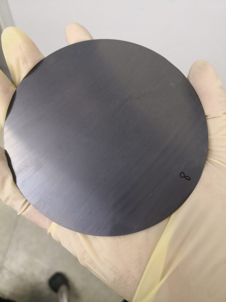
Standard 4‑inch silicon wafers normally feature thickness between 500 μm ~ 800 μm. In the semiconductor industry, silicon substrates ≥1 mm are defined as ultra‑thick silicon wafers. Specially‑customized ultra‑thick wafers can reach up to 4 mm, which are non‑standard non‑stock items requiring dedicated production runs.
Ultra‑thin silicon wafers generally range from 5 μm to 100 μm, widely adopted for high‑end semiconductor thinning processes. Wafers thinner than 50 μm are regarded as extra‑thin grade; we can deliver products down to 5‑20 μm.
Ultra‑flat silicon wafers are precision‑grade silicon substrates with TTV ≤3 μm, strictly‑controlled low Bow & Warp to minimize wafer deformation under free‑state conditions.
| Wafer Type | Core Technical Challenges | Key Control Parameters | Typical Applications |
|---|---|---|---|
| 4 mm Ultra‑Thick Silicon Wafer | Chuck offset under self‑weight, cumulative grinding stress | TTV, edge chipping, mechanical strength | High‑voltage substrates, thermal dissipation base, deep silicon etching |
| Ultra‑Thin Silicon Wafer (<100 μm) | Poor rigidity, high risk of warpage & cracking | Temporary bonding, low‑stress grinding | Power device thinning, TSV advanced semiconductor packaging |
| Ultra‑Flat Silicon Wafer | Internal stress, global thickness uniformity, zero free‑state warpage | TTV / Bow / Warp 3‑D flatness, surface uniformity | High‑precision photolithography, wafer bonding, thin‑film deposition, metrology calibration substrates |
Main Applications of Ultra‑Thick, Ultra‑Thin & Ultra‑Flat Silicon Wafers
Ultra‑Thick Silicon Wafer Applications
- High‑voltage power semiconductor substrates: for high‑voltage thyristors, rectifiers and high‑power IGBT test substrates. Thick silicon wafers deliver larger voltage‑withstand insulation distance and superior heat dissipation. Uniform thickness guarantees even force distribution during pressure‑contact packaging and prevents local stress‑induced device burnout.
- Optical windows & infrared detector substrates, laser optical carriers: monocrystalline silicon shows excellent infrared transmittance. Thick‑silicon substrates provide high mechanical strength and minimal thermal deformation for infrared optical windows and optical carrier platforms.
- Scientific‑research experimental platforms: high‑temperature CVD / PECVD coating substrates, high‑voltage electrical‑test carriers, mechanical‑strength validation samples and thermal dissipation test specimens.
- Thermal‑management carrier substrates: silicon features outstanding thermal conductivity. Ultra‑thick silicon wafers can serve as passive heat‑dissipation bases for miniature components.
Ultra‑Thin Silicon Wafer Applications
Power Semiconductor Devices: common thickness:30‑120 μm, mainstream 50‑80 μm. Thinned silicon shortens vertical current conduction paths, reducing on‑resistance (Rdson) by 15%‑30% and switching loss. Thermal resistance drops significantly, heat‑dissipation efficiency improves over 50%, lowering chip temperature rise and extending power‑cycle service life.
Advanced Semiconductor Packaging (TSV / 3D Stacking, 2.5D Interposer, WLCSP): typical thickness:20‑50 μm. Applied for HBM high‑bandwidth memory, multi‑layer 3D NAND stacking and Chiplet heterogeneous integration for AI computing chips. Shortens wiring routes and reduces signal delay & power consumption.
WLCSP & Fan‑out Packaging: enables ultra‑thin chip form‑factors for mobile processors and RF baseband chips, supporting compact device profiles together with RDL redistribution layers for high‑density pin layout.
Silicon Interposer: ultra‑flat ultra‑thin silicon wafers at 20‑30 μm act as transition substrates between logic chips and high‑bandwidth memory for high‑performance computing platforms.
Back‑Side Illuminated CMOS Image Sensor (CIS): mass‑production thickness 20‑40 μm. Circuits are fabricated on the front‑side, while the wafer is fully thinned from back‑side to allow light to penetrate silicon and reach PN photodiodes.
MEMS Micro‑Electro‑Mechanical Systems (4/6‑inch ultra‑thin wafer core market): working thickness 30‑80 μm; specialized micro‑structure products down to 10‑30 μm. Used for accelerometers, gyroscopes, pressure sensors, silicon‑based microphone diaphragms. Thinner silicon improves mechanical sensitivity and resonant performance. Also suitable for microfluidic chips and infrared MEMS thermal‑sensing chips.
RF & Millimeter‑Wave Devices (20‑50 μm): wafer thinning suppresses substrate parasitic capacitance and RF signal loss. Optimized for millimeter‑wave radar, 5G RF front‑end chips and Bluetooth RF modules to enhance high‑frequency signal stability.
| Thickness Range | Positioning | Typical Applications |
|---|---|---|
| 80‑120 μm | Industrial‑grade thin silicon wafer | Conventional IGBT, general‑purpose MEMS, photovoltaic cells |
| 30‑80 μm | Mass‑production ultra‑thin grade | EV automotive IGBT, CIS image sensors, RF semiconductor chips |
| 20‑30 μm | High‑end extra‑thin custom | TSV stacking, HBM interposer, premium back‑illuminated CIS |
| <20 μm | Lab‑grade / frontier flexible electronics | Flexible electronics, implantable medical devices, special R&D custom substrates |
Ultra‑Thin Silicon Wafer Specification Table
Supports custom ultra‑thin silicon wafers with customized special processes. Thickness can be tailored according to customer requirements.
| Diameter | Type | Thickness | TTV | Bow | Warp | Surface Finished | Packing |
|---|---|---|---|---|---|---|---|
| 50.8 mm (2″) | P / N | 50 μm‑100 μm | ≤10 μm | ≤30 μm | ≤30 μm | SSP, DSP, PIG | Wafer Carrier |
| 100 mm (4″) | P / N | 50 μm‑200 μm | ≤10 μm | ≤30 μm | ≤30 μm | SSP, DSP, PIG | Wafer Carrier |
| 150 mm (6″) | P / N | 80 μm‑300 μm | ≤10 μm | ≤30 μm | ≤30 μm | SSP, DSP, PIG | Wafer Carrier |
| 200 mm (8″) | P / N | 100 μm‑500 μm | ≤10 μm | ≤30 μm | ≤30 μm | SSP, DSP, PIG | Wafer Carrier |
| 300 mm (12″) | P / N | 100 μm‑500 μm | ≤10 μm | ≤30 μm | ≤30 μm | SSP, DSP, PIG | Wafer Carrier |
Related Products: A‑R‑M special orientation sapphire substrates, InP substrates, GaAs wafers, custom ultra‑thick silicon wafers, ultra‑flat silicon wafers.
Previous Article: Anisotropic hardness characteristics of crystal orientations for silicon wafers Next Article: Testing instruments for wafer defects including TTV, Warp, Bow, particle contamination and scratches.