
what is soi wafers?Overview
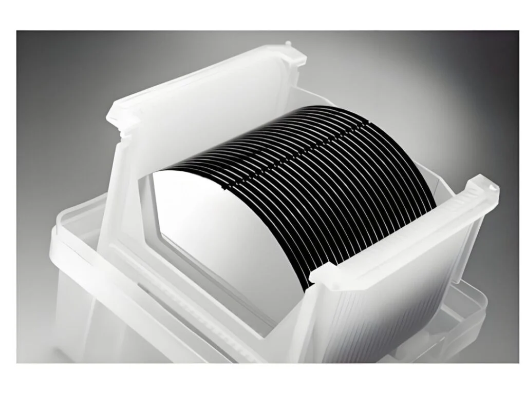
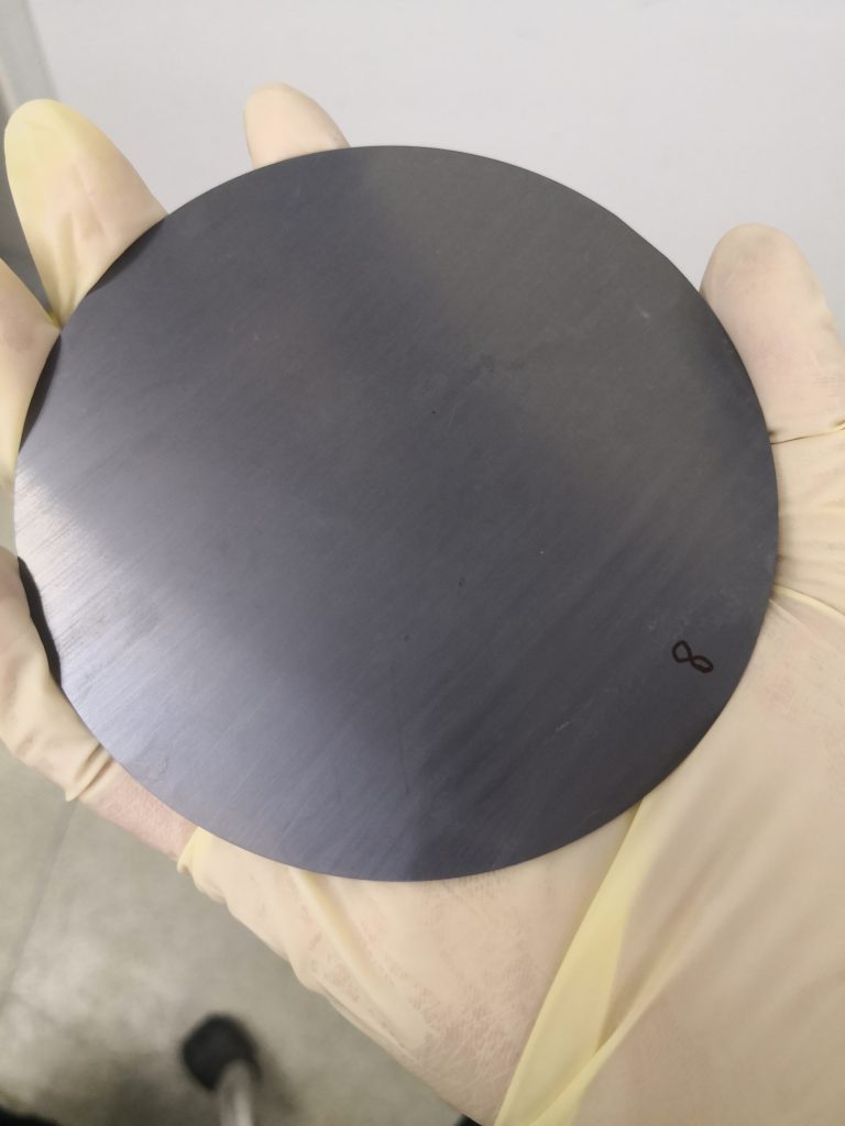
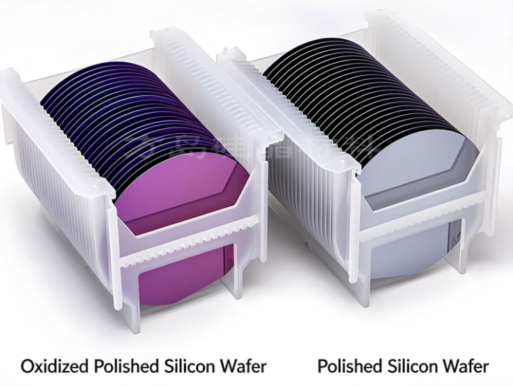
SOI (Silicon‑On‑Insulator) wafers are high‑performance monocrystalline silicon substrates widely adopted for advanced high‑end semiconductor chips. Monocrystalline silicon ingots go through slicing, lapping and polishing to produce bare polished silicon wafers. Polished wafers can be further processed via epitaxy to make epitaxial wafers. By applying oxidation, wafer‑bonding or ion‑implantation processes, polished silicon wafers are converted into finished SOI wafers.
Bare polished silicon wafers can be directly fabricated into semiconductor devices for memory chips and power‑semiconductor components. Power semiconductors are designed for high‑voltage and large‑current operating conditions without device breakdown. As high‑power operation generates considerable heat which may trigger component failure, power‑device design focuses on lowering power loss and improving heat dissipation efficiency.
As IC manufacturers pursue higher integration density, faster operating speed and lower power consumption, conventional bulk‑silicon structures fail when devices are scaled down to sub‑micron nodes. This drives the development of the SOI architecture, where active silicon devices are built upon thin monocrystalline silicon layers grown over insulating substrates.
Originally proposed for sub‑micron CMOS devices to replace bulk‑silicon and SOS (Silicon‑On‑Sapphire) architectures, SOI technology has evolved into a mainstream solution for high‑speed integrated circuits and partial 3D‑IC implementations, and remains a hot research topic for modern semiconductor‑material engineering.
Key Advantages of SOI Structure
Dielectric isolation delivers low parasitic capacitance, which is highly beneficial for high‑speed, high‑density integrated circuits.
Dielectric isolation reduces electrical noise and significantly improves radiation‑hardening performance of circuits and devices.
Effectively suppresses CMOS latch‑up failure.
Compared with SOS substrates, SOI wafers feature superior crystal quality and broader application coverage. For CMOS circuits, SOI can reduce mask layers and eliminate isolation‑diffusion steps to simplify layout and boost integration density. SOS suffers thermal‑expansion mismatch between silicon and sapphire, introducing compressive stress within silicon thin‑films. Meanwhile, SOI delivers lower power consumption and lower substrate cost than SOS, while SOS cannot support 3D‑device architectures.
Multiple SOI manufacturing techniques have reached commercial maturity. Further improvements in process control and material quality will expand real‑world deployment; certain SOI variants support 3D‑IC manufacturing.
二、SOI Wafer Specifications
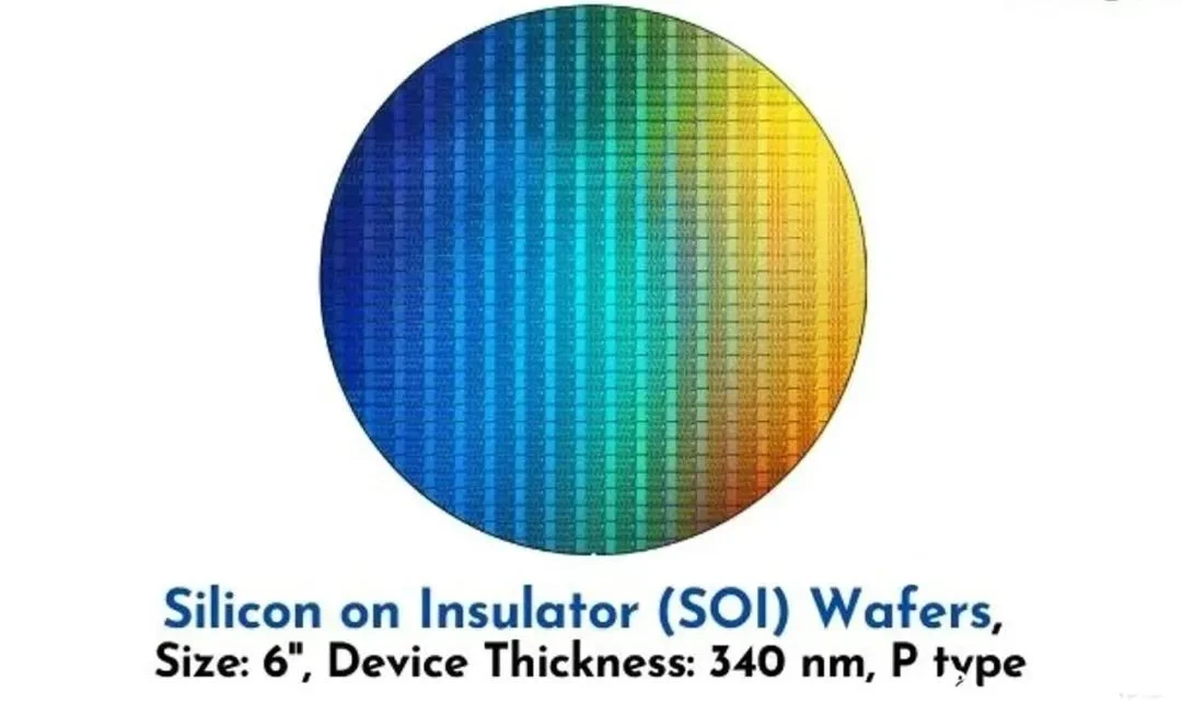
| Item | Parameter |
|---|---|
| Wafer Diameter | 4″ / 5″ / 6″ / 8″ |
| Device Layer | |
| Dopant | Boron, Phosphorus, Arsenic, Antimony, Undoped |
| Crystal Orientation | <100>, <111> |
| SOI Technology Type | SIMOX, BESOI, Simbond, Smart‑cut |
| Resistivity | 0.001‑20000 Ohm‑cm |
| Device‑Layer Thickness | 0.2‑150 μm |
| Thickness Uniformity | <5 % |
| BOX (Buried Oxide) Layer | |
| BOX Thickness | 0.4‑3 μm |
| BOX Uniformity | <2.5 % |
| Handle Substrate | |
| Substrate Orientation | <100>, <111> |
| Dopant / Type | P‑Type(Boron), N‑Type(Phosphorus), N‑Type(As), N‑Type(Sb) |
| Substrate Thickness | 300‑725 μm |
| Substrate Resistivity | 0.001‑20000 Ohm‑cm |
| Surface Finish | P/P, P/E |
| Particle Contamination | <10 @0.3 μm |
Main SOI Manufacturing Technologies
1. Lateral Melting Recrystallization
This process forms an SiO₂ dielectric layer over a silicon handle wafer, followed by deposition of amorphous or poly‑silicon. Localized melting and zone‑moving recrystallization transform deposited silicon into monocrystalline thin‑film. Major branches include laser‑beam recrystallization, electron‑beam recrystallization, graphite‑strip seeded lateral recrystallization and illumination‑melting recrystallization. Each approach differs in heating hardware, processing conditions and final material performance, with respective pros and cons. This technology was widely studied in early‑stage SOI research.
2. Epitaxial Lateral Over‑Growth (ELO / CVD Lateral Growth)
ELO is a mature CVD‑based SOI manufacturing method evolved from selective epitaxy. Photolithography opens seed windows on SiO₂ masking layers; silicon epitaxy initiates inside seed openings while nucleation over SiO₂ is suppressed. After filling seed windows, silicon grows laterally across the dielectric surface with optimized lateral‑to‑vertical growth ratio.
The core challenge lies in restraining poly‑silicon nucleation on SiO₂ surfaces. A repeated growth‑and‑HCl‑etch cycle removes unintended silicon deposits on dielectrics, enabling continuous large‑area monocrystalline silicon films with target thickness. Material quality approximates conventional epitaxial silicon, yet residual poly‑crystalline nuclei and limited lateral span remain technical bottlenecks. Process temperature runs 1050 ℃‑1150 ℃, well below silicon melting temperature and minimizing substrate dopant redistribution, making ELO promising for 3D‑IC fabrication.
3. SIMOX (Separation by Implanted Oxygen)
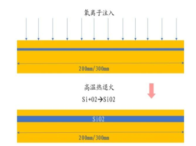
SIMOX fabricates buried SiO₂ layers via high‑dose oxygen‑ion implantation. Typical implantation dosage ranges 1.2‑1.8×10¹⁸ ions/cm². Buried‑oxide depth correlates with implantation energy: ~500 keV yields ~0.5 μm BOX depth; 1 MeV yields ~1 μm BOX depth.
Slightly excess implantation dosage (>1.8×10¹⁸/cm²) is recommended for sharp Si‑SiO₂ interfaces; insufficient dosage generates twin defects at upper interfaces. Post‑implant high‑temperature annealing (1150‑1250 ℃ for 2 hours) drives chemical reaction between silicon and implanted oxygen, repairs ion‑implant crystal damage and forms continuous buried‑oxide layers. Pre‑depositing a thin SiO₂ capping layer before annealing reduces surface defects and improves annealing outcomes.
SIMOX features simple workflows and full compatibility with standard silicon‑device manufacturing processes, yet it cannot support 3D‑device architectures.
4. Wafer‑Bonded SOI (Bonding‑Etch‑Back SOI / BESOI)
Bonding‑based SOI technology bonds two polished silicon wafers. One wafer carries thermally‑grown silicon‑dioxide, then joins the second silicon wafer. Thermal treatment enables siloxane‑bond adhesion across the contact interface. Back‑side grinding, etching and CMP thin down the donor wafer to reach the target device‑layer thickness, completing the SOI stack structure.
Bonded SOI delivers straightforward processing workflows, yet strict flatness requirements for paired wafers are mandatory for full‑interface contact, and donor‑wafer thinning remains technically challenging. This bonding‑based approach keeps rapid development momentum in industry.
Simbond Technology
Simbond combines strengths of SIMOX and wafer‑bonding workflows. Oxygen ions are implanted into one silicon wafer followed by high‑temperature annealing to create buried oxide. This wafer is then bonded to a second handle substrate, then receives secondary high‑temperature annealing to form high‑quality bonding interfaces. CMP thinning stops automatically upon reaching the buried‑oxide stop‑layer, delivering highly uniform device‑layer thickness.
Both SIMOX SOI and Bonded‑type SOI possess distinct process principles, performance characteristics and application scenarios. Material selection shall be determined according to practical application requirements and manufacturing constraints.
Typical Applications
- CMOS Integrated Circuits
- Memory Chips
- Power Semiconductor Devices
- MEMS & Sensor Components
- Radiation‑Hardened Electronic Devices
- High‑Speed & Radio‑Frequency Semiconductor Chips
Inquiry
Contact us for custom SOI wafer quotation. We provide SIMOX, BESOI, Smart‑Cut and Simbond SOI substrates with customizable device‑layer / BOX‑layer thickness across 4‑8 inch sizes.
more:SOI晶圆 4inch 5inch 6inch 8inch——高品质半导体材料的领先供应商 SOI Wafer (Silicon‑On‑Insulator Wafer)