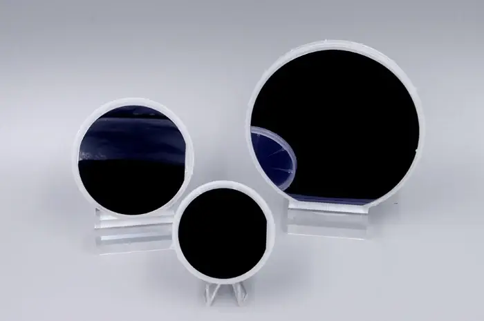

Overview
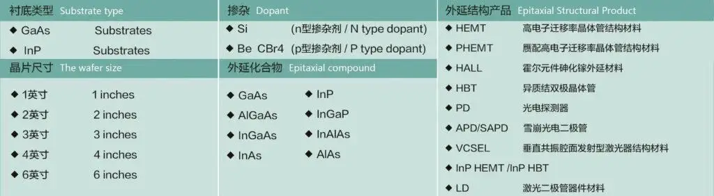
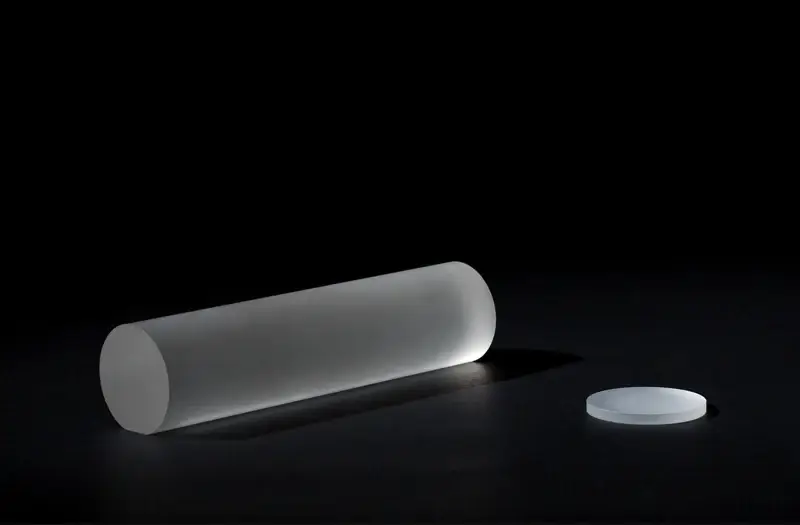
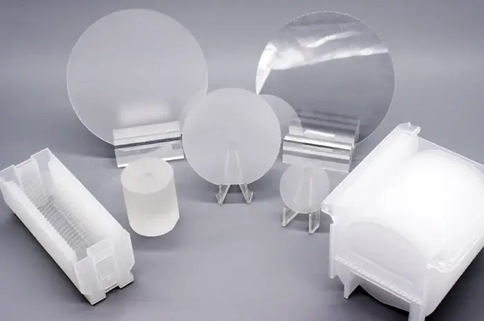
Gallium Arsenide (GaAs) is one of the most established and important III‑V compound semiconductor materials, widely deployed in optoelectronic and micro‑electronic industries.
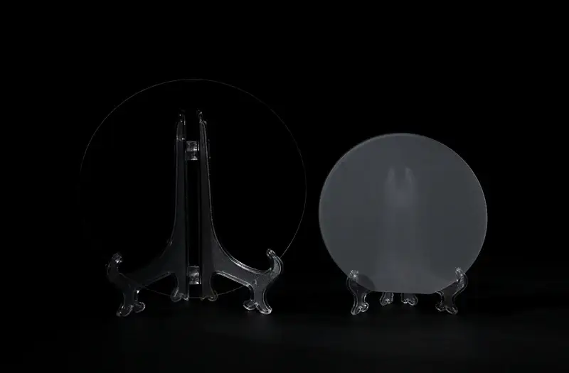
GaAs substrates fall into two major categories: semi‑insulating GaAs and conductive GaAs.
- Semi‑insulating GaAs is mainly used for integrated circuits built with MESFET, HEMT and HBT structures. Typical applications cover radar systems, microwave & millimeter‑wave communication, ultra‑high‑speed computers and optical‑fiber communication.
- Conductive GaAs serves for semiconductor laser diodes (LD), light‑emitting diodes (LED), near‑infrared lasers, quantum‑well high‑power lasers and high‑efficiency solar cells.
Fundamental Physical & Chemical Properties of GaAs
GaAs features a direct band‑gap with double‑valley energy‑band structure. Its crystal appears dark‑grey with metallic luster.
- Chemically, it is insoluble in hydrochloric acid at room temperature, reacts with concentrated nitric acid, and dissolves readily in aqua regia. It remains stable under water vapor and oxygen atmosphere.
- Oxidation starts at 600 °C, and thermal dissociation occurs above 800 °C.
Lower effective mass brings higher electron velocity. The electron effective mass of GaAs equals 1/15 of free‑electron mass and 1/3 of silicon’s electron effective mass. Transistors manufactured from GaAs achieve 3‑4 times faster switching speed compared with silicon‑based counterparts.
GaAs delivers high electron mobility and high saturation drift velocity. Under low‑electric‑field conditions, its electron mobility reaches approx 8500 cm²/(V·s), far exceeding silicon. As electric‑field intensity rises, electron drift velocity climbs to a peak value and then declines.
Another core merit is its semi‑insulating property. Even after area ion implantation, the substrate can maintain internal electrical isolation, which makes it ideal as IC‑grade substrate material. Devices fabricated on semi‑insulating GaAs feature low parasitic capacitance, well‑suited for high‑speed components such as monolithic microwave integrated circuits (MMIC).
Main Application Fields
1. Optoelectronics
GaAs can be directly processed into optoelectronic devices including LED chips, visible‑light lasers, near‑infrared lasers and quantum‑well high‑power lasers.
GaAs laser diodes have prominent strengths: compact form‑factor (e.g. portable small‑size battlefield radar powered by GaAs laser, delivering pulse width of 1.0×10⁻¹¹ s and output power up to 6 W), long service life and large communication capacity. A single GaAs laser enables transmission for thousands of voice channels in optical communication links.
2. Micro‑electronics
Based on semi‑insulating GaAs substrate, self‑aligned planar technology with direct ion implantation fabricates GaAs high‑speed digital ICs, microwave monolithic ICs, optoelectronic integrated circuits and high‑power FETs. These components are characterized by fast speed, high frequency, low power consumption and radiation‑resistance. They are critical for national defense equipment, civil industries and national infrastructure construction.
Driven by booming consumer wireless communication and smartphone markets in recent years, semi‑insulating GaAs substrates for high‑frequency communication devices have seen rapid market expansion.
3. Microwave Industry
Compared with silicon microwave devices, GaAs microwave devices provide higher output power, higher operating frequency, higher gain and lower noise under relatively low supply voltage. GaAs FET and avalanche diodes work at dozens of gigahertz and have potential to exceed 100 GHz, which is of great significance for radar and microwave communication systems. High gain and low‑noise features greatly improve sensitivity of microwave systems.
GaAs Gunn diodes operate at supply voltage ranging from 5 V‑7 V, allowing compact, lightweight power supplies, which is highly valuable for aerospace applications.
4. Solar Cells
GaAs is a promising candidate for high‑efficiency solar‑cell fabrication. Commercially dominant silicon solar cells reach conversion efficiency of 18%‑20%, while GaAs solar cells can achieve projected efficiency of 23%‑26%. GaAs solar cells feature superior radiation‑hardening capability and stable performance under high‑temperature operating environments.
Related Products: GaN Substrate, Silicon Wafer, Sapphire Wafer 2英寸砷化镓衬底