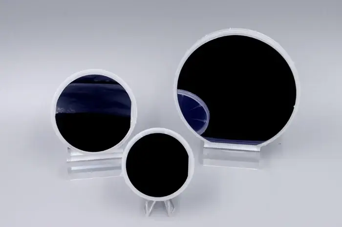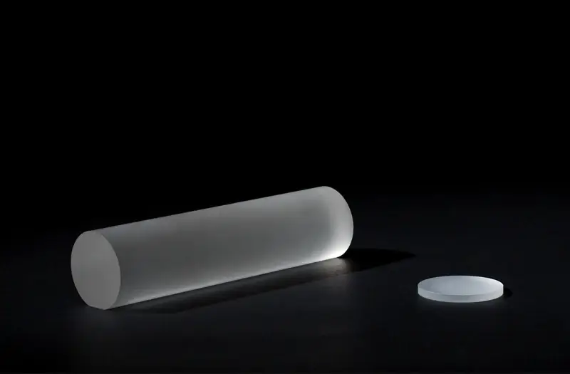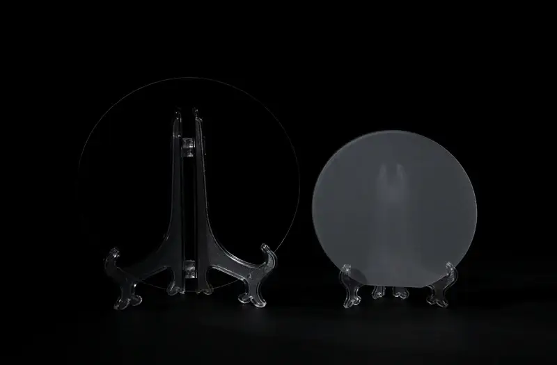
C‑Plane Single‑Crystal Sapphire Substrate
C‑plane single‑crystal sapphire substrate is manufactured from high‑purity α‑Al₂O₃ with a hexagonal lattice structure. Featuring excellent chemical stability, it is insoluble in water and highly resistant to strong acids and alkalis. With a Mohs hardness of 9, melting point of 2050 °C and boiling point of 3500 °C, its maximum operating temperature can reach 1900 °C. This sapphire wafer delivers outstanding optical transmittance, thermal conductivity, electrical insulation and mechanical performance, with prominent wear‑resistant and scratch‑proof properties, making it an ideal epitaxial base for optoelectronic and semiconductor devices.
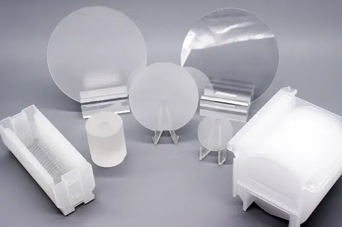
Main Applications of C‑Plane Sapphire Substrate
Our epi‑ready C‑plane sapphire wafers are widely adopted across multiple high‑tech industries:
- GaN‑based LED lighting & display: Core substrate for high‑brightness LED chips, Micro‑LED epitaxy growth.
- Laser Diodes: Blue light and ultraviolet laser diode manufacturing.
- RF Communication Devices: Key material for 5G communication modules and radar components.
- Power Electronic Devices: Applied in new‑energy vehicle power units and industrial power supply systems.
Besides standard C‑plane sapphire substrates, we also supply A‑plane, M‑plane, R‑plane and special off‑angle customized sapphire substrates to meet diverse R&D and mass‑production requirements.
| Item | Parameter |
|---|---|
| Material | >99.99% High‑purity Mono‑crystalline Al₂O₃ (KY method) |
| Diameter | 25.4 mm, 50.8 mm, 76.2 mm, 100 mm, 125 mm, 150 mm, 200 mm, 300 mm |
| Thickness | 500 μm, 430 μm, 500 μm, 650 μm, 800 μm, 1000 μm, 1200 μm, 2000 μm |
| Crystal Orientation (C‑plane 0001) | Off‑angle toward M‑axis (10‑10): 0.2 ±0.1°;
Off‑angle toward A‑axis (11‑20):0 ±0.1°; For 12‑inch wafer:0 ±0.5° |
| Primary Flat Orientation | A‑Plane (11‑20) ±1.0° |
| Primary Flat Length | 8 mm /16 mm /22 mm /30 mm /30 mm /47.5 mm; large size for notch design |
| Front‑Side Surface | Epi‑polished, Ra<0.3 nm (1‑8 inch); Ra<0.5 nm (12 inch) |
| Back‑Side Surface | SSP: Fine‑ground Ra=0.8‑1.2 μm;DSP: Epi‑polished Ra<0.3 nm (1‑8 inch); DSP Ra<0.5 nm (12 inch) |
| Laser Marking Side | Back‑side (not available for 12‑inch wafer) |
| TTV(Total Thickness Variation) | ≤5 μm ~ ≤30 μm (diameter dependent) |
| BOW | ≤8 μm ~ ≤45 μm (diameter dependent) |
| WARP | ≤10 μm ~ ≤60 μm (diameter dependent) |
| Edge Exclusion | ≤2 mm (1‑8 inch), ≤3 mm (12‑inch) |
Note: Custom off‑cut angles, special thickness, notch/flat configuration and strict flatness parameters are supported for customer‑oriented projects.
Why Choose Our C‑Plane Sapphire Wafers
 Ultra‑high purity raw material >99.99% monocrystalline Al₂O₃, low dislocation density for high‑quality GaN epitaxy growth.
Strict control of TTV, Bow & Warp parameters, stable batch consistency for mass production.
Two surface options available: SSP (single‑side polished) and DSP (double‑side polished), epi‑ready finish for direct epitaxial process.
Wide size range from 1‑inch research sample up to 12‑inch large‑diameter production wafers.
Flexible customization: special crystal orientation, miscut angle, thickness and edge treatment for laboratory R&D and industrial manufacturing.
If you want to get quotation, datasheet or sample of C‑plane single‑crystal sapphire substrate, please feel free to contact us. We provide professional technical support and global shipment service for semiconductor and optoelectronic customers.
FAQ
Q1: What is C‑plane sapphire substrate used for?
A: C‑plane (0001) sapphire wafer is the mainstream substrate for GaN‑based LED, laser diodes, RF components and power electronic devices.
Q2: What is SSP and DSP for sapphire wafer?
A: SSP stands for Single‑Side Polished, DSP for Double‑Side Polished. Customers can select surface finish according to their epitaxy process.
Q3: Can you supply custom off‑angle sapphire substrates?
A: Yes. We support customized off‑cut towards M‑axis or A‑axis, together with special thickness and notch/flat requirements.
Transparent Polished Sapphire Tube Custom Wall Thickness | High Purity Al₂O₃ Sapphire Tube Supplier 12 Inch FZ High Resistivity Silicon Wafer | Float‑Zone Substrate 4‑Inch Custom Ultra‑Thick Silicon Wafers|Custom Ultra‑Thin & Ultra‑Flat Silicon Wafers C向蓝宝石单晶衬底 okwafer|提供优质蓝宝石衬底