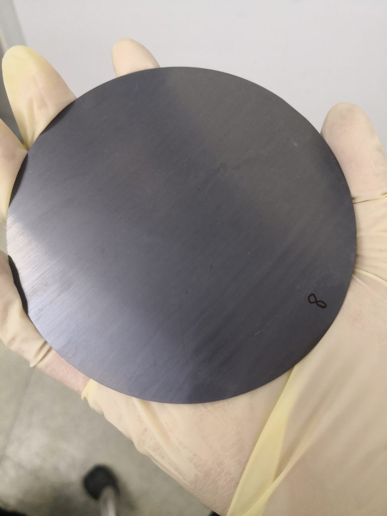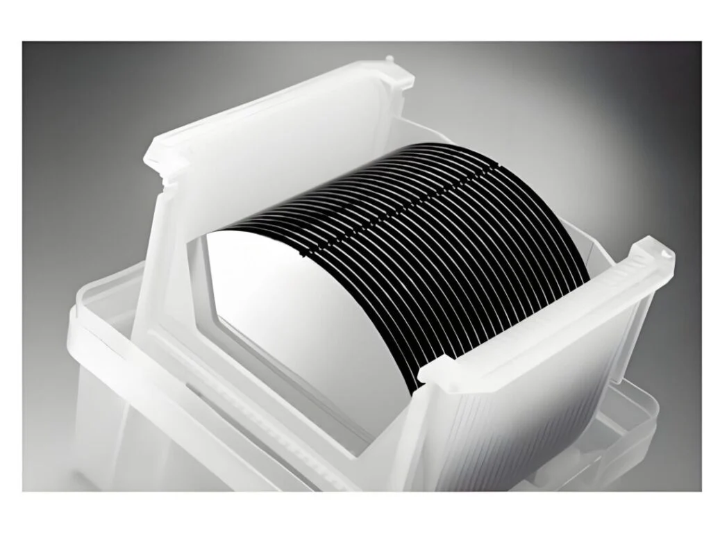

hat is 12‑Inch (300 mm) FZ High‑Resistivity Silicon Wafer?
FZ stands for Float‑Zone crystal growth technology. Float‑zone silicon is grown without contact with quartz crucibles, delivering extremely low oxygen and carbon impurities.
High‑resistivity FZ silicon typically features resistivity ≥ 1000 Ω·cm. Standard Czochralski (CZ) silicon cannot reach such ultra‑high‑resistivity ranges. It is an essential substrate material for RF circuits and high‑voltage power semiconductor devices.
The 12‑inch (300 mm) format represents a high‑end large‑diameter specification for float‑zone wafers, with far more difficult mass‑production requirements compared to 6‑inch and 8‑inch FZ silicon wafers.
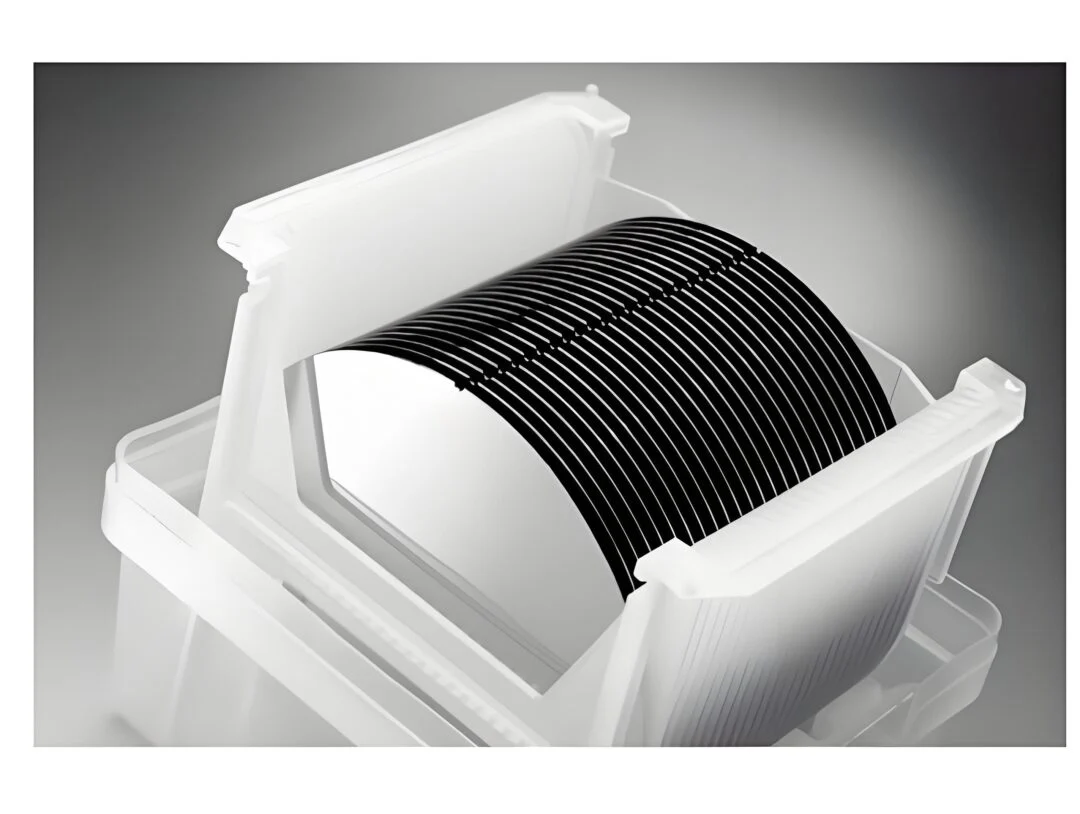
Market Reference Price for 12‑Inch FZ High‑Resistivity Silicon Wafers
Note: All figures are market reference values; actual prices will fluctuate according to specifications, grades, order quantity and lead‑time.
- Intrinsic undoped ultra‑high‑resistivity FZ wafer (> 10 kΩ·cm, for RF & terahertz applications) Domestic lab & small‑batch supply: USD 1,250 – USD 2,200 per piece. Imported prime‑grade original wafers: USD 2,500 – USD 3,900 per piece. Single‑piece sample from overseas spot channels may exceed USD 3,000 per wafer.
- Test‑grade / lapped wafer (R&D prototyping, non‑strict particle control) NTD neutron‑doped high‑resistivity lapped wafer: USD 310 – USD 540 per piece. Intrinsic ultra‑high‑resistivity lapped wafer: USD 760 – USD 1,240 per piece.
For comparison: conventional lightly‑doped 12‑inch CZ polished silicon wafer costs only USD 95 – USD 125 per unit.
The price of 12‑inch FZ high‑resistivity silicon wafer can reach 6‑30 times that of standard CZ wafer. Major contributing factors include very low yield of large‑diameter FZ single‑crystal ingots, limited NTD neutron‑transmutation‑doping capacity, and extreme challenges for full‑wafer uniformity control.
Key Comparison: 12‑inch CZ vs 12‑inch FZ High‑Resistivity Silicon
| Parameter | 12‑inch Czochralski (CZ) Silicon | 12‑inch Float‑Zone (FZ) High‑Resistivity Silicon |
|---|---|---|
| Oxygen Content | 20‑45 ppma | < 0.1 ppma |
| Maximum Resistivity | ≤ 200 Ω·cm | Up to 20 000 Ω·cm |
| Breakdown Voltage | Moderate | Extremely high |
| High‑Frequency Loss | High | Ultra‑low for RF applications |
| Minority‑Carrier Lifetime | Relatively short | Extra‑long; low leakage current |
| Cost & Production Volume | Low‑cost, mass‑production | High‑cost, small‑batch specialty production |
| Typical Use Cases | Logic chips, memory devices, general low‑voltage power semiconductors | RF devices, radar systems, ultra‑high‑voltage power devices, terahertz systems |
Main Applications of High‑Resistivity FZ Silicon Wafers
- RF & Microwave Communication 5G RF front‑end chips, radar and satellite transceiver chips. High‑resistivity substrates deliver low dielectric loss and suppress signal cross‑talk.
- High‑Voltage Power Semiconductors 650 V‑3300 V IGBT, super‑junction MOSFET, high‑voltage rectifiers and thyristors.
- Optoelectronics, Infrared & Terahertz Systems Infrared optical windows, terahertz spectrometers, optical sensors. Float‑zone silicon features good mid‑to‑far‑infrared transmittance.
- Specialty Semiconductor Sensors High‑voltage Hall‑effect sensors and particle radiation detectors.
- High‑Frequency Dummy / Calibration Substrates Reference dummy wafers for RF probe‑station calibration and process qualification.
Related Articles
- Float‑Zone FZ Silicon Wafers — Latest Supply Status
- CZ vs FZ Silicon Wafers: Specifications, Price and Difference
- Platinum‑Coated Silicon Wafer: Why Deposit Metal Films on Silicon
- 6‑Inch FZ High‑Resistivity Silicon Wafer Pricing