1. What are Vicinal / Off‑Cut Substrates
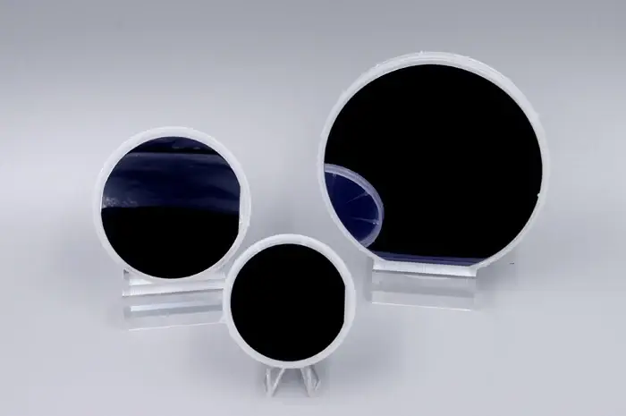
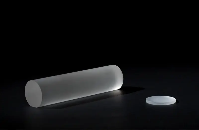
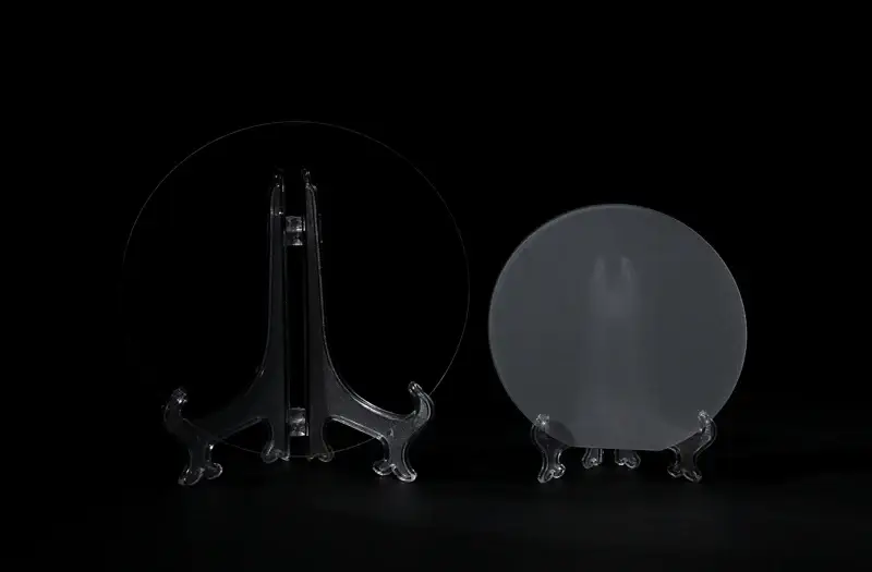
Off‑Cut Single‑Crystal Sapphire Substrates:Vicinal substrates, also known as off‑cut, miscut or off‑axis single‑crystal substrates, are monocrystalline wafers intentionally sliced with a small tilt angle (typically 0.5°‑10°) relative to standard low‑index crystal planes such as sapphire C‑plane, SiC (0001) or β‑Ga₂O₃ (100). This intentional mis‑orientation generates periodic atomic step‑terrace structures on wafer surfaces, which precisely regulate epitaxial growth modes and improve crystal quality for semiconductor epitaxy.
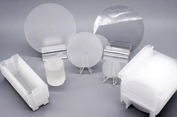
2. Core Advantages of Off‑Cut / Vicinal Substrates
- Reduction of dislocation density: Guiding atomic arrangement along surface steps and suppressing dislocations caused by lattice mismatch. For instance, GaN grown on 5° off‑cut sapphire achieves roughly 1/3 lower dislocation density compared with on‑axis flat substrates.
- Polarity & crystal orientation tuning:
- Sapphire: C‑plane off‑cut for polar GaN growth; A‑plane / R‑plane off‑cut enables semi‑polar or non‑polar GaN, improving LED efficiency and wavelength stability.
- SiC: Specific off‑cut angles eliminate hexagonal hillock defects of N‑polar GaN, drop dislocation density down to 10⁸ cm⁻² and nearly double breakdown voltage.
- Defect suppression: β‑Ga₂O₃ (100) substrate off‑cut 4° along [00‑1] direction exposes (−201) step surfaces to eliminate twin defects, supporting high‑voltage power devices with breakdown field up to 2.7 MV/cm.
- Superior surface morphology: Step‑flow epitaxy delivers surface roughness close to original substrate, enhancing device uniformity and production yield.
3. Common Off‑Cut Materials & Typical Parameters
Other custom single‑crystal vicinal substrates are available upon inquiry.
| Item | Specification |
|---|---|
| Material | >99.99% High‑purity mono‑crystalline Al₂O₃ (KY method) |
| Crystal Orientation Options | C‑axis (0001): off‑cut 0.5°‑10° ±0.1° toward M‑axis (1‑100)
C‑axis (0001): off‑cut 0.5°‑8° ±0.1° toward A‑axis (11‑20) A‑axis (11‑20): off‑cut 0.5°‑6° ±0.1° toward M‑axis (1‑100) A‑axis (11‑20): off‑cut 0.5°‑6° ±0.1° toward C‑axis (0001) R‑axis (1‑102): off‑cut 0.5°‑6° ±0.1° toward M‑axis (1‑100) R‑axis (1‑102): off‑cut 0.5°‑6° ±0.1° toward C‑axis (0001) M‑axis (1‑100): off‑cut 0.5°‑6° ±0.1° toward C‑axis (0001) |
| Diameter | 50.8 mm (2 inch), 100 mm (4 inch), 150 mm (6 inch) |
| Standard Thickness | 430 μm (2″), 650 μm (4″), 1000 μm (6″) |
| Primary Flat Orientation | A‑plane ±0.3° |
| Primary Flat Length | 16 mm (2″), 30 mm (4″), 47.5 mm (6″) |
| Front‑Side Finish | Epi‑polished, Ra<0.3 nm (epi‑ready surface) |
| Back‑Side Finish | SSP: Fine‑ground, Ra 0.8‑1.2 μm; DSP: Epi‑polished, Ra<0.3 nm |
| Total Thickness Variation (TTV) | <10 μm (2″); <20 μm (4″); <25 μm (6″) |
| BOW | −15~0 μm (2″); −25~0 μm (4″); −35~0 μm (6″) |
| WARP | <15 μm (2″); <30 μm (4″); <40 μm (6″) |
| Edge Exclusion | ≤ 2 mm |
5. Key Selection Guidelines for Vicinal / Off‑Cut Substrates
- Off‑cut angle selection
- Small angle (0.5°‑2°): Wider atomic terraces, suitable for thick‑film epitaxy with ultra‑smooth surface.
- Medium angle (2°‑6°): Balanced step density and defect suppression, most widely adopted for mass‑production epitaxy.
- Large angle (>6°): Dense atomic steps, ideal for ultra‑thin‑film growth and polarity control, with slightly increased surface roughness.
- Off‑cut direction: Decides step alignment and exposed crystal facets, directly controls epitaxial polarity and defect modes. For sapphire substrates, off‑cut toward A‑axis and M‑axis produce completely different epitaxy performance.
Contact & Customization
Custom special‑orientation single‑crystal vicinal substrates are supported. Welcome to send inquiry for datasheet, quotation and technical consultation.
4‑Inch Custom Ultra‑Thick Silicon Wafers|Custom Ultra‑Thin & Ultra‑Flat Silicon Wafers C‑Plane Sapphire Substrate | High Purity α‑Al₂O₃ Wafer for LED & Power Electronics 12 Inch FZ High Resistivity Silicon Wafer | Float‑Zone Substrate Silicon Thermal Oxide Wafer 蓝宝石偏角度单晶衬底-斜切角晶向衬底 A-R-M特殊晶向蓝宝石衬底